A Lithium Battery Charger with Load Sharing
You may have found that charging your project’s lithium battery while at the same time trying to use your circuit didn’t quite workout, with problems like the circuit not turning on and the battery never finish charging. Even an LED can cause the battery to never finish charging.
This article goes through creating a battery charger with load sharing (also known as power-path) that can properly charge the battery and have the main circuit run normally. The charging IC we’ll be using is the popular MCP73831/2 from Microchip for single-cell Li-Po and Li-Ion batteries with a maximum charge current of 500mA.
We’ll also be adopting the load sharing design from Microchip app note AN1149.
Issues when not using load sharing
During the preconditioning and constant-current charge phases the charger IC will limit current supplied to the battery and load. If this limit has been set to 40mA and the load wants 30mA, only 10mA will be left to charge the battery. If the load wants 50mA then 40mA will come from the charger and 10mA from the battery, which will discharge the battery rather than charge it. If the battery is already dead then the load will be starved of current, causing the voltage to drop, the load probably won’t operate correctly and the battery won’t charge.
During the constant-voltage charge phase the charger will normally wait until the current through the battery is below a particular percentage (usually 7.5% of the set charge current) and then finish charging. If a load is present the current will probably never go below this level and charging will never seem to finish.
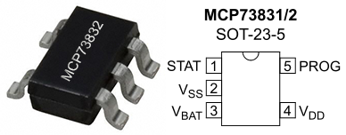
Charger IC variations
There are a few variations of the charging IC, MCP73831/2 refers to MCP73831 and MCP73832. The only difference between these two is the charging state output (STAT pin).
| Charge state | MCP73831 | MCP73832 |
|---|---|---|
| Shutdown | Hi-Z | Hi-Z |
| No battery present | Hi-Z | Hi-Z |
| Preconditioning | Low | Low |
| Constant-current fast charge | Low | Low |
| Constant voltage | Low | Low |
| Charge complete – standby | High | Hi-Z |
There are also variations which set how the battery is charged in relation to when and how long to precondition, fast charge and so on. AC, AD, AT and DC are the 4 types. The AC type seems to be the ‘normal’ type that is used in the IC datasheet. More information about each charging phase can be found in the app note above.
Basic Charge Circuit
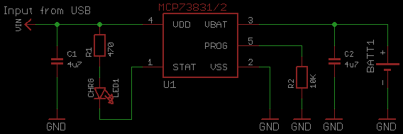
This design is the minimum required for the MCP73831/2 to charge a lithium battery (well, R1 and LED1 could also be removed), but problems will arise when charging and connecting a load to the battery, as discussed above.
Charge circuit with load sharing
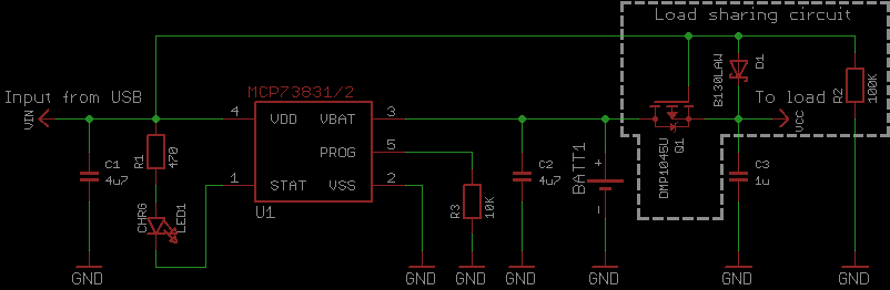
Adding load sharing only requires an additional 3 components. When USB power is applied this circuit will turn off Q1, and as long as (Vusb – D1 VF) is above (Vbat – Q1 VSD) then the load will instead use power from USB through D1. This allows the battery to charge normally without any outside disturbances.
Q1 is a P channel MOSFET. When USB power is applied Q1 will turn off and stop current flowing from the battery to the load, effectively disconnecting the battery. The load will then use power from USB through D1. The MOSFET you choose should have as low RDS(on) as possible to minimize power loss, should be able to handle the current your circuit is going to draw from the battery and has a VGS(th) between 0V and -2.4V.
D1 is to prevent current flowing from the battery into the charging power source. D1 should be a schottky diode that can handle the loads’ maximum current draw. The forward voltage drop doesn’t matter too much, but lower the better to reduce power loss when powered by USB. The absolute maximum drop is (VINmin – (VBATmax – VSD) = VFmax), the USB 2.0 standard specifies 5V±0.25V, most lithium batteries charge to 4.2V and internal MOSFET diodes have a drop of around 0.6V, so (4.75 – (4.2 – 0.6) = 1.15). This maximum forward voltage drop is so the source (load side) voltage of Q1 doesn’t go below the drain (battery side) voltage, otherwise the internal diode of Q1 will begin to conduct which will interfere with the battery charging. Reverse current leakage of schottky diodes might be a problem if ultra low power consumption is needed.
R2 is to make sure Q1 turns on and connects the battery to the load when the charging power source is removed.
C3 is an extra decoupling/bypass capacitor.
Another important point to think about is the reverse leakage current of D1, which could be up to a few hundred microamp (schottky diodes are very leaky).
This leakage current will create a small voltage at the MOSFET gate which, if high enough, could cause the MOSFET to not turn back on properly when the main Vin power is removed.
To see if Q1 is turning on properly place a voltmeter across Q1’s drain and source pins and it should read a few millivolt depending on load and the MOSFET’s on resistance, e.g. with a load of 100mA and RDS(on) of 50mΩ then the voltage drop should be 5mV.
To minimize the gate voltage you can either use a diode with lower leakage current (which will also improve battery life) or reduce the value of R2, or a bit of both.
To figure out what value R2 should be to keep the gate voltage to a sane level (lets go for a Vtarget of 1V) we first workout the effective resistance D1 has at the batteries’ max voltage:
Our example diode has a leakage (IR) of 200uA @ 4.2V (you can find leakage info in the datasheet for your diode, or you can measure it yourself by applying a voltage backwards across the diode and measuring the current).
RD = VBATmax / IR
RD = 4.2 / 0.0002
RD = 21KΩ
So now we can treat D1 and R2 as a voltage divider, we just need to workout what value R2 should be so that the voltage at the MOSFET’s gate meets our Vtarget.
R2 = Vtarget * RD / (VBATmax – Vtarget)
R2 = 1 * 21000 / (4.2 – 1)
R2 = 6.56KΩ
So when using a diode with a leakage current of 200uA @ 4.2V, R2 must be no more than 6.56K to keep the MOSFET’s gate at 1V. I’d recommend not going over 100K for R2.
This also means D1 and R2 will be leaking a total of 152uA from the battery (I = VBATmax / (RD + R2)).
It’s probably a good idea to do these calculations for VBATmin (around 2.4 – 3V) too.
Charge circuit with load sharing and additional microcontroller
Here’s an even further modified charge circuit. A microcontroller can be used to sense when USB power is applied, when the battery is charging, enable/disable charging, control charge rate and measure the battery voltage. This information could be displayed on something like an LCD.
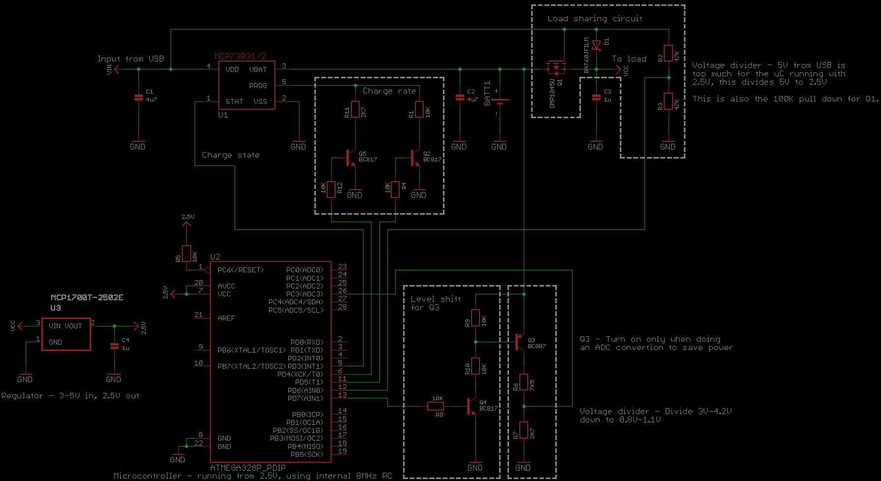
| Pin | I/O | Pull-up | Info |
|---|---|---|---|
| PD3 (5) | Input | Enabled | Charger STAT pin sense. LOW means the battery is charging. |
| PD6 (12) | Input | Disabled | When USB power is applied this pin will go HIGH. |
| PD4 (6) | Output | - | Controls charging. |
| PD5 (11) | Output | - | Controls charging. |
| PD7 (13) | Output | - | Setting to HIGH will turn the level shifter and Q3 on which will allow current to flow through the divider. Once an ADC reading has been taken this should be put back to LOW. |
| ADC3 (26) | ADC | - | Measure voltage. Internal 1.1V should be used as the reference voltage. |
Charge rates
| Q2 | Q5 | Charge current |
|---|---|---|
| Off | Off | Disabled |
| On | Off | 100mA (10k) |
| Off | On | 370mA (2.7k) |
| On | On | 470mA (2.7k || 10k = 2.126k) |
R2 and R3 voltage divider also serves as R2 100K pull-down resistor for Q1 in the first load sharing schematic.
Only the MCP73832 should be used in this case, using MCP73831 will drive the STAT pin HIGH with 5V when the battery finishes charging which will exceed the microcontrollers’ max pin voltage of VCC + 0.5V (2.5 + 0.5 = 3V max).

Extra
- You should make sure your circuit can run on the full voltage range of the battery (usually 3V-4.2V, but sometimes down to 2.4V) as well as 5V from USB.
- You should make sure that your charging power source can supply enough current to charge the battery as well as power the circuit.
- When charging at high currents be sure to have large enough PCB traces to dissipate the heat from the charging IC. Heat comes from the ground pin (VSS).
June 13th 2014 – Updated microcontroller schematic to use more suitable BJTs instead of MOSFETs (cheaper, easier to find). Also added adjustable charge rate.

Comments